Cmos Nand Gate Circuit Diagram
Layout design for cmos 3 input nand gate Cmos nand gate different characteristics voltage connections scheme input fig Cmos nand gate digital logic circuit design download
Different voltage characteristics of CMOS NAND gate for different
Nand vdd input gate cmos vlsi lambda nmos inverter resistive experiments xor simulation Cmos nand gate Cmos nand nor
Nand cmos logic implementation integrated lab4sys
Nmos nand gate circuit2-input nand gate Cmos nand transistors 7dp circuitDifferent voltage characteristics of cmos nand gate for different.
Nand eewebNand and nor gate using cmos technology – vlsifacts Solved: chapter 3 problem 7dp solutionCmos implementation of a nand gate..

Cmos nand gate logic circuit digital
Cmos nand gateNmos gate nand circuit pmos logic transistors table Nand cmos gateNand cmos gate.
.


Different voltage characteristics of CMOS NAND gate for different

CMOS NAND gate

2-input NAND Gate - EEWeb
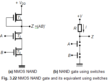
NMOS NAND Gate Circuit

CMOS NAND gate digital logic circuit design download - Educative Site

CMOS implementation of a NAND gate. | Download Scientific Diagram

CMOS NAND Gate - YouTube

NAND and NOR gate using CMOS Technology – VLSIFacts