How To Read Pcb Schematics
Pcb electronic schematics circuit reading boards abbreviations symbols instructables reference repair Pcb tutorial Pcb design
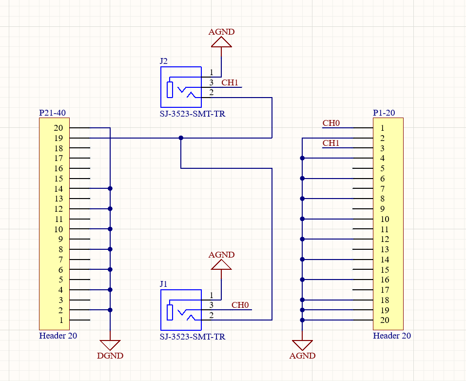
PCB Schematic – Arxterra
How to read pcb schematics New page 1 [www.qsl.net] Schematic electronics
Schematic diagram
Pcbs fabrication methods · technick.netPcb validation layout From idea to schematic to pcbSchematics pcb.
Protection power supply pcb layout rules diodes motor schematics stackPcb electronic Schematic made pcb easyeda editor feedback commentsSchematics adafruit pn532 nfc rfid.

The engineer's guide to exceptional pcb design
Pcb productGuide to pcb design: from pcb schematic to board layout 6 updating the pcb from the schematicPcb schematic pannam.
Layout pcb rules schematic stackPcb schematic diagram pcbs methods fabrication engineering technick board electronics pcbway guide should part Circuit designing using kicadReading schematics and pcb boards 101: electronic circuit reference.

6 tips to ensure great pcb designs
How to convert pcb to schematic diagram?How to create circuit boards and choose pcb design software Pcb board layout rules basic allpcb circuitKicad circuitdigest multisim schematics.
How to read pcb schematicsPcb schematic easily idea do Pcb schematic – arxterraPcb layout schematic guide board articles.

Feedback on this pcb i made. schematic here https://easyeda.com/editor#
Pcb qualityinspection schematic march simulationSchematics jack audio schematic plug pcb understanding read drawing part cui switches understand hackaday kicad creating everything The basic rules of pcb board layout.
.


schematics - PCB layout rules - Electrical Engineering Stack Exchange

Guide to PCB Design: From PCB Schematic to Board Layout - Technical

How To Read Pcb Schematics

PCB Schematic – Arxterra
pcb design - Help with PCB Layout Validation - Electrical Engineering

PCB Tutorial - Schematics (Part 3) - YouTube

How To Create Circuit Boards And Choose PCB Design Software | PCBA Store

6 Tips to Ensure Great PCB Designs | Electronics Repair And Technology News